One long-standing headache for designers has been how to efficiently switch back and forth between different design tools and manufacturing processes. It's like an architect juggling multiple blueprint software programs, each requiring different formats and rules; if every time you had to redraw everything from scratch, not only would it waste time, but paperwork would drag innovation to a crawl. Cambridge-based Wave Photonics wants to break this cycle of "repetitive labour." They've launched a new PDK management platform (Process Design Kit management system) that acts like a master key, unlocking all the doors and allowing designers to move freely between different design environments without constantly transferring materials.
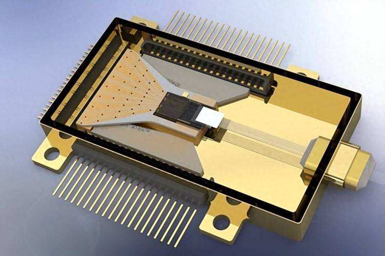
In practice, chip designers rely on "process design kits" (PDKs) provided by foundries. Think of a PDK as the construction manual for building a house-it contains detailed parameters of materials, usable tools, foundations you can lay, and which structures are safe. The problem is, this "manual" must be readable, but designers use a wide variety of software: some rely on Luceda, others on Cadence, and many use the open-source GDSFast. The result is that each foundry has to spend a great deal of time translating this manual into multiple "languages" to make it compatible with those tools. It's like taking the same instruction book, and translating it into English, French, German, and Spanish, then constantly updating each version. This repetitive work consumes massive amounts of energy, forcing designers to spend time on setup and adaptation instead of focusing on true innovation.
Wave Photonics' platform is designed to solve this pain point. It seamlessly connects foundry PDKs with mainstream design tools, automatically handling all the "translation" and "adaptation" tasks. Once a designer receives a PDK, they can immediately use it within their preferred software, without extra configuration. It's like giving architects worldwide a universal translator; no matter what language you speak, your blueprints are instantly understandable, and the platform can even generate simulation data automatically. What's more, it can help foundries automatically generate critical simulation parameters (S-parameters), enabling designers to quickly verify whether circuits will function properly. In effect, it's like having a "virtual laboratory" built right next to your blueprints.
Confidentiality is a big deal in the semiconductor industry. A foundry's process details are like secret recipes; once leaked, the consequences can be disastrous. Wave Photonics' platform balances efficiency with security by incorporating fine-grained access control. Imagine the entire PDK as an encrypted archive, while the platform serves as a vault with tiered permissions. Only authorised users can access certain folders, and every interaction is logged to prevent "misuse" or "mix-ups." This means foundries can safely distribute PDKs globally without fear of leaks, while designers always receive the latest version, avoiding more awkward situations of "building a house with outdated blueprints."
For photonic chip designers, the impact is immediate: no more spending weeks on repetitive format conversions and software adaptations. With a PDK in hand, they can get straight to work. Automated document management and version control eliminate the risk of using outdated files. It's like designers reclaiming two hours every day once spent on paperwork, and redirecting that time toward genuine creativity and breakthroughs.

Wave Photonics' platform may never shine like a consumer product in the public eye, but its role is more like the highways beneath a city— unassuming yet essential. Without such "infrastructure," even the brightest designers would be bogged down in a swamp of file conversions and version chaos. Now, they finally have a clear. Smooth road ahead, freeing up energy to explore the limitless possibilities of the photonic world. At its core, Wave Photonics' PDK management platform is a collaboration tool that liberates both designers and foundries.